 Hey Guys! Hope you’re well. I welcome you on board. In this post today, I’ll walk you through PCBA (Printed Circuit Board Assembly) in detail.
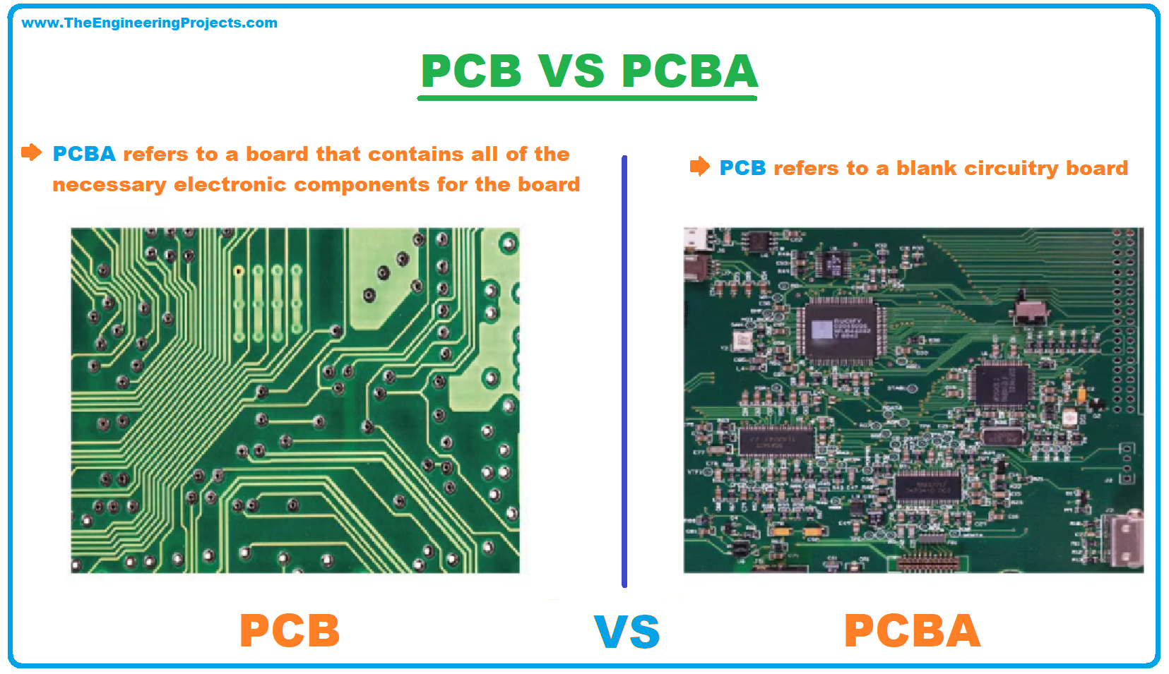
A printed circuit board (PCB) provides physical support and electrical connection through conductive copper layers for the electronic components placed on the board. When you get the finished PCB, it is just a board without electrical components. PCB with the electrical components on the board turns to PCBA which is PCB with the assembly attached. You can place and connect these components yourself if you know how to solder them on the board, or you can outsource this service to the company for the smooth insertion of these components on the boards without compromising the quality of the PCB.
Curious to know more about PCBA?
Keep reading.
JLCPCB Fabrication House for PCBA
- JLCPCB is a an excellent PCB fabrication manufacturer that also provides PCBA service for successfully mounting the electronic components on the PCBs.
- From solder paste printing and SMT to reflow soldering and optical inspection, the board goes through every step with careful scrutiny, ensuring top quality finished PCB assembled with electronic components.
- You’ll never regret picking JLCPCB for meeting your electronic needs.
- If you’re looking for reliable and economical PCBA service, you should give JLCPCB Fabrication house a try.
PCBA Definition
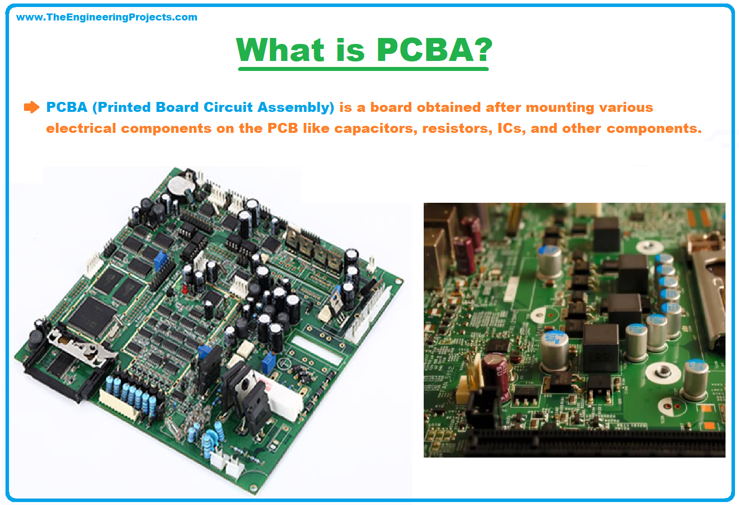
- PCBA (Printed Board Circuit Assembly) is a board obtained after mounting various electrical components on the PCB like capacitors, resistors, ICs, and other components based on the application.
- A PCBA normally passes through a reflow furnace heating to develop a mechanical connection between the components and the PCB.
PCBA Manufacturing Process
- Several steps are involved in the Printed Circuit Board Assembly manufacturing process.
- Each step must be in harmony with the next one to ensure a seamless production process for getting the quality final product.
The PCB undergoes DFM (design for manufacturability) check before the actual PCBA process even starts. The DFM check cross-checks the final PCB structure with the initial blueprint of the design. This check identifies any missing links or potentially redundant and problematic features in the final PCB design.
If PCB doesn’t undergo this check, the PCBA process can create trouble in properly mounting the components on the board and maintaining a flawless electrical connection between them. DFM checks not only reduce the cost of the manufacturing process but also ensure the overall functionality of the PCB.
PCBA production process comes with the following steps.
-
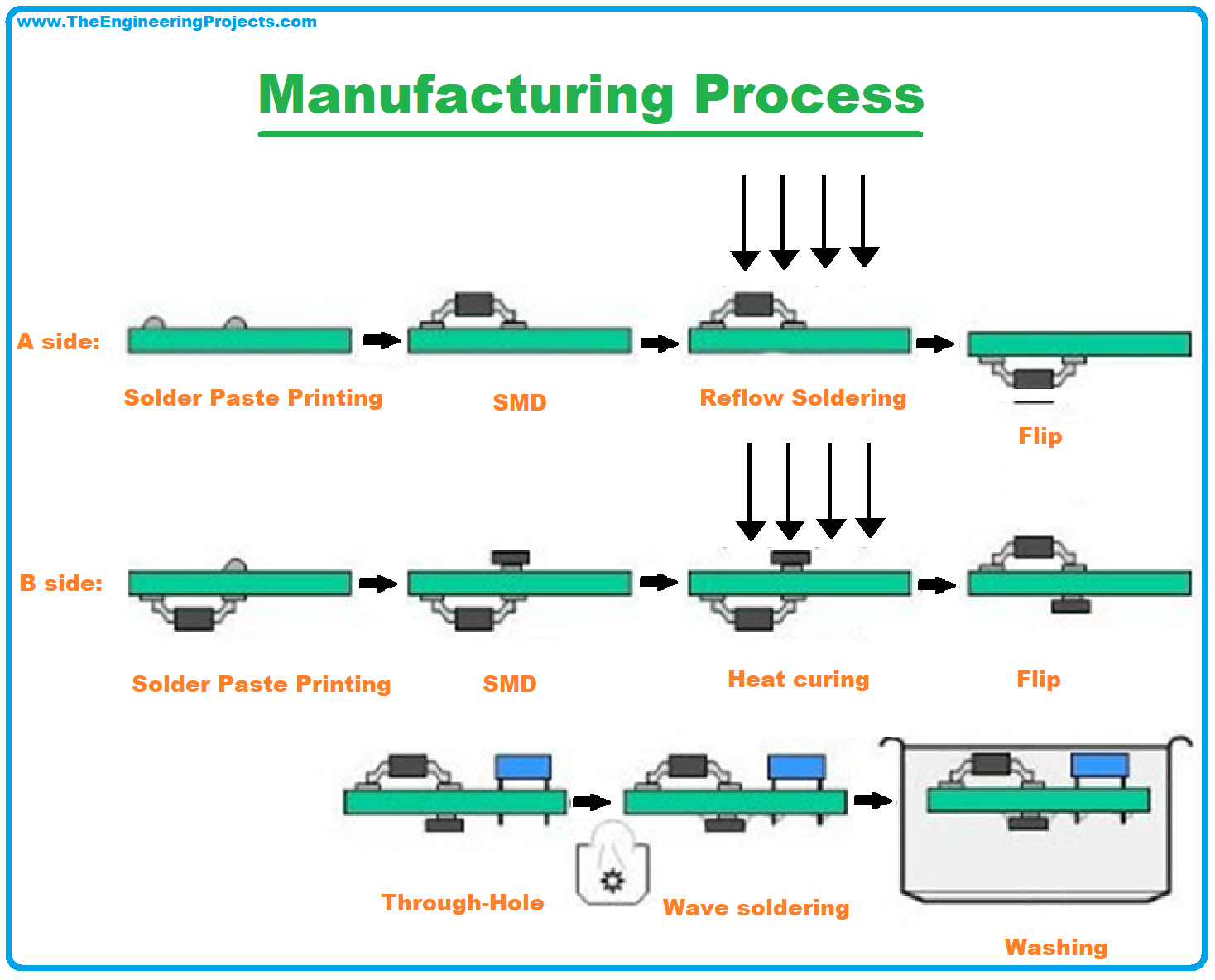
Solder Paste
Before adding components on the board, a solder paste is added to the areas where components rest on the finished PCB. The solder paste comes with greyish tiny balls of metals, also called solder. The solder paste is mixed with the flux that turns to a chemical composition that must be added in the right amounts in the right areas on the board.
To add the solder paste, a mechanical fixture is used to hold both the PCB and solder stencil in place. An applicator then takes the solder paste in precise amounts and places it on the desired PCB areas. The machine then rolls the solder paste evenly on the intended PCB areas. As the stencil is removed, the solder paste sits on the desired areas.
-
SMT Assembly
After properly adding the solder paste on the board, the board is then passed through the pick and place process where the robotic machine is used to pick the surface mount components from the reels and place them on the intended areas of the board.
The components added remain in the desired areas due to the sticky feature of the solder paste. The solder paste comes with enough bond strength that keeps the components in place.
Earlier this procedure was practiced manually by humans. However, the inception of advanced technology removed the need for this erratic manual process, since the automated process by machines is more accurate and efficient than the traditional manual process.
-
Reflow Soldering
Once the electronic components have been placed in the desired locations they remain there due to the presence of solder paste. The board then undergoes a Reflow Soldering process that solidifies the solder paste to keep the components at the required areas.
In this process, the finished board is transferred to a conveyer belt that passes through a big reflow oven that comes with a series of heaters; the temperature of these heaters stays around 250 C which generates gradual heat to bake the board. At this stage, the temperature is high enough that allows the solder to melt in the solder paste, keeping the components tightly in place.
Once the solder has been melted down, the finished product is then passed through a series of cooler heaters that cools down the melted solder paste, giving it strength and creating a permanent solder joint to firmly connect the surface mount components with the board.
This is the reflow soldering for the one-sided PCB. Know that for two-sided PCB the stenciling and reflowing will be done separately for each side.
-
Inspection
Once the reflow soldering has been done, the assembled board undergoes a proper inspection where the functionality of the board is tested. As the PCB passes through a reflow soldering process, it may result in poor connection quality or in worst cases, the elimination of the entire connection. To check these problematic features and common errors, the assembled board undergoes a careful inspection.
- Optical Inspection: Recognize that, manual inspection is not an option for inspecting hundreds of surface mount components on the boards, instead, automatic optical inspection is exercised to look for the defects and errors in the board. In optical inspection, an automatic optical machine is used that comes with high-powered cameras that are located at different angles to monitor the connections. The solder connections reflect light at high speed with different intensities, allowing the machine to analyze the connections of lower quality.
- X-Ray Inspection: For complex and layered circuit boards, the x-ray inspection method comes into play where x-rays are used for the inspection. With x-rays, layers become transparent, helping you see through the layers and identify the common problems on the board. These inspections are carried out before the final functional test inspection that involves the steps to make sure the board is fully functional and does the job perfectly.
-
Plated Through Hole Components
Based on the type of board the components used, the components assembly goes beyond the scope of SMT components insertion. In that case, Plated Through Hole (PTH) components insertion is used where holes are drilled on the board that go completely through the board establishing a conductive path from one side of the board to another. Solder paste is not used in this case because it won’t stick and creeps into the drilled holes. In this PTH process, two types of soldering processes may be used:
- Manual Soldering: This soldering is manually done by humans. In this process, one person at the station is given a task to insert components on the desired PTH area. Once finished, the board is transferred through a conveyer belt to another station where another person is destined to insert another component. The cycle continues until each hole is filled with the desired component.
- Wave Soldering: Wave soldering is an automatic process that is slightly different than manual soldering. Once the PTH component is placed on the desired hole area, the board is transferred through a conveyer belt that passes through a special oven that smears the layer of melted solder on the bottom of the board, soldering all pins at once at the bottom of the board.
-
Functional Test
In this process, the finished product undergoes the final inspection called ‘functional test’ where simulated and power signals run through the PCB to analyze the electrical characteristics of the board. If voltage, current or signal output in these characteristics show sudden fluctuation beyond the permitted range, it means the board has failed the test.
-
Feedback
It is important to investigate any failures to guarantee the functionality of the manufacturing process. The recommended place to monitor the output and the potential errors is the optical inspection stage. Since if errors are detected and rectified at this stage, this may save you time and money and keep you from producing boards with similar defects.
PCBA Pricing
- The price of the PCBA is obviously more than the manufacturing of the standard circuit board. Since in PCBA, electrical components are mounted on the PCB using SMT technology.
- The size of the circuit board and the number of components that need to be mounted on the board play a key role in defining the overall cost of the assembled circuit boards.
- Moreover, the size of the holes and the total number of holes are also important factors while defining the price of the board.
- Similarly adding more layers to the board and the type of material used will influence the cost.
- The customization in the manufacturing process will affect the cost; the more custom features you would like to add to the board, the more the cost.
That’s all for today. Hope you’ve enjoyed reading this article. If you have any questions, you can pop your comments in the section below. I’d love to help you the best way I can. Thank you for reading the article.
JLCPCB – Prototype 10 PCBs for $2 (For Any Color)
China’s Largest PCB Prototype Enterprise, 600,000+ Customers & 10,000+ Online Orders Daily
How to Get PCB Cash Coupon from JLCPCB: https://bit.ly/2GMCH9w
The post PCBA: Definition, Types, Material, Manufacturing Process, Price & Applications appeared first on The Engineering Projects.


No comments:
Post a Comment