 Hello Friends! Hope you’re well today. I welcome you on board. In this post today, I’ll walk you through the Introduction to 2SC1061.
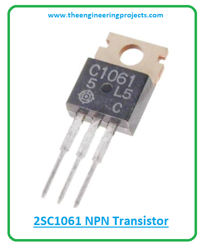
2sc1601 is an NPN bipolar junction transistor used for switching and amplification purposes. During the amplification process, the small input current across one pair of terminals is used to generate a large output current across other pairs of terminals.
2sc1601 is known as a semiconductor device made of silicon material. This is a bipolar junction transistor where two charge carriers (electrons and holes) play an important role in the conductivity inside the transistor. As this is an NPN transistor so here major charge carriers are electrons while holes are the minority carriers.
I suggest you buckle up as I’ll detail the complete Introduction to 2SC1061 covering datasheet, pinout, features, and applications.
Let’s dive in.
Introduction to 2SC1061
- 2sc1601 is a power transistor used for amplification and switching purposes. It comes with two junctions i.e. base-collector junction that is reverse biased and base-emitter junction that is forward biased.
- This bipolar junction transistor belongs to the NPN transistor family where electrons are the major charge carriers.
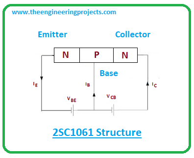
- This chip is made of three layers where one p-doped layer stands between the two n-doped layers.
- 2sc1601 contains three terminals named emitter, base, and collector. These terminals are used for the external connection with the electrical circuit.
- Both collector-emitter and collector-base voltages are 50V while the emitter-base voltage is 4V which is the amount of voltage needed to bias the transistor and initiate the transistor action.
- The DC current gain ranges from 35 to 320 which is the value of current this transistor can amplify. This current gain is based on the current and voltage characteristics of the transistors.
2SC1061 Datasheet
It is wise to go through the datasheet before you incorporate this device into your project. The datasheet comes with the main characteristics of the device, helping you better understand the absolute maximum ratings of the device. Click the link below to download the datasheet of 2sc1601.
2SC1061 Pinout
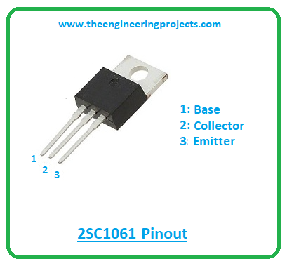
The 2sc1061 contains three pins named:
1: Base
2: Collector
3: Emitter
The following figure shows the pinout diagram of transistor 2sc1061.
- All these terminals contain different doping concentrations. The collector pin is lightly doped while the emitter terminal is highly doped compared to other terminals.
- The collector pin is 10-times less doped compared to the base pin. Moreover, the emitter side carries the entire current of the device. Because current on the emitter side is the combination of both collector current and base current.
- Plus, NPN transistors are preferred over PNP transistors for a range of applications because the mobility of electrons is far better and quicker than the movement of holes.
2SC1061 Working Principle
- The working of this transistor is simple and straight forward. When a positive voltage is applied at the base terminal, it gets biased and the current starts flowing from the collector to the emitter pin.
- Both electrons and holes play a vital role in the conductivity process inside the transistor but electrons are majority carriers and holes are minority carriers.
- It is important to note that bipolar junction transistors are not symmetrical components. Which projects that exchanging the collector and emitter terminals will keep the transistor from working in forward active mode and as a result, both terminals will start working in the reverse active mode. This can influence the values of common-emitter current gain and common-base current gain.
- Different doping concentrations of both emitter and collector terminals are responsible for the lack of symmetry inside the transistor.
- The Common-emitter current gain of this device is 35-320 in this transistor, which is denoted by beta and the common-base current gain is always less than one which is denoted by alpha.
2SC1061 Alternatives
The complementary PNP transistor to this NPN transistor is 2SA671.
And the equivalent to 2SC1061 is MJC32C.
Double-check the pinout of the alternative before incorporating it into your project as the pinout of alternative might differ from the pinout of 2SC1061.
2SC1061 Power Ratings
The following table shows the absolute maximum ratings of 2sc1601.
| Absolute Maximum Ratings of 2SC1061 | ||||
|---|---|---|---|---|
| Pin No. | Pin Description | Pin Name | ||
| 1 | Collector-emitter voltage | 50V | ||
| 2 | Collector-base voltage | 50V | ||
| 3 | Base-emitter voltage | 4V | ||
| 4 | Collector current | 3A | ||
| 5 | Power dissipation | 25W | ||
| 6 | Base current | 0.5A | ||
| 7 | Operating and storage junction
temperature range |
-55 to 150C | ||
- The collector-emitter and collector-base voltages are 50V. And total power dissipation is 25W which shows the amount of power released during the functioning of this device. The junction temperature and storage temperature ranges from -55 to 150C.
- When you’re working with the component, make sure the ratings don’t exceed the absolute maximum ratings. Otherwise, they can badly damage the device, thus the entire project.
- Moreover, don’t apply these ratings more than the required time, else they can affect device reliability.
2SC1061 Applications
2sc1061 is employed in the following applications.
- Employed to support loads under 3A.
- Incorporated in modern electronic circuits.
- Used in Bistable and Astable multivibrators circuit.
- Used in voltage regulator circuits.
- Used for switching and amplification purpose.
- Employed in the switched-mode power supply.
- Installed in the motor control circuit.
- Used in H-bridge circuits.
2SC1061 Physical dimensions
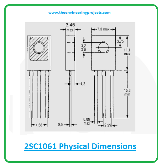
The following figure represents the physical dimensions of the 2sc1061 device.
By checking the physical dimensions of this component you can evaluate the space required for your circuit and install the device accordingly.
That’s all for today. Hope you find this article helpful. If you are unsure or have any questions, you can pop your comment in the section below, I’m ready and happy to assist you the best way I can. Feel free to share your valuable suggestions and feedback around the content we share so we keep coming back with quality content customized to your exact needs and requirements. Thank you for reading the article.
JLCPCB – Prototype 10 PCBs for $2 (For Any Color)
China’s Largest PCB Prototype Enterprise, 600,000+ Customers & 10,000+ Online Orders Daily
How to Get PCB Cash Coupon from JLCPCB: https://bit.ly/2GMCH9w
The post 2SC1061 NPN Transistor Datasheet, Pinout, Features & Applications appeared first on The Engineering Projects.


No comments:
Post a Comment