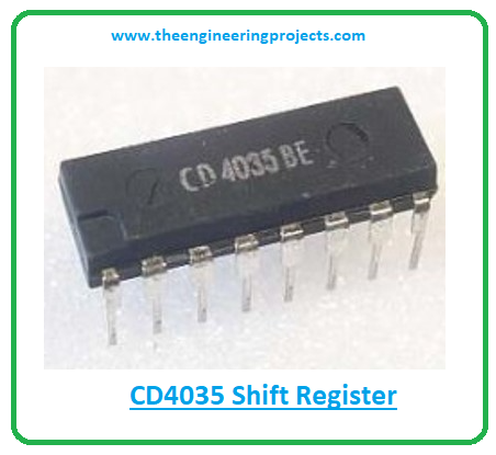
 Hello Everyone! Hope you’re well today. Happy to see you around. In this post today, I’ll walk you through the Introduction to CD4035.
The CD4035 is a shift register that is mainly used in counters, control circuits, and registers. It contains clocked signal serial chip that is a four-stage register. Synchronous Parallel inputs are provided to each stage and serial inputs are offered to the first stage via JK logic.
I suggest you read this post all the way through as I’ll detail the complete introduction to CD4035 covering datasheet, pinout, features, alternatives, and applications.
Let’s jump right in.
Introduction to CD4035
- The CD4035 is a shift register that is a 16-pin device and is mainly used in control circuits, counters, and registers.
- It is a four-stage register that comes with synchronous parallel inputs provided to each stage and is available in 16-pin PDIP, GDIP, PDSO packages.
- The CD4035 chip contains two 4-bit Parallel In – Parallel Out Shift Registers which projects that it is used to receive (input) data-parallel and can control 4 output pins in parallel.
- Simply put, it extracts data from four parallel inputs, and as a result, shifts them and then offers that data on four parallel outputs.
- It carries the clock input edge that is used for data shifting where data is shifted on every positive clock edge.
- This four-stage register stage comes with D Flip Flops in each stage that are connected with each other.
- This chip seems to be the right fit for the applications where microcontrollers don’t have enough GPIO pins to handle the number of outputs.
- Since this chip can operate as the data bit for LCD, CD4035 can be employed for interfacing LCD screens
- The frequency of this chip is 12MHz at Vdd = 10V and the propagation delay time is 500ns.
- While the operating voltage range is 3V to 18V and the operating temperature range is -55C to 125C.
CD4035 Datasheet
Before you integrate this component into your electrical project, it’s wise to go through the datasheet of the component that details the main characteristics of the device. Click the link below and download the datasheet of CD4035.
CD4035 Pinout
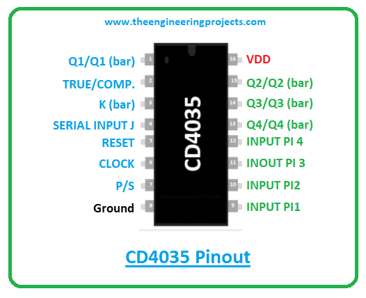
The following figure shows the pinout diagram of CD4035.
The following table shows the pin number, name, and description of each pin incorporated on the chip.
| Pin Description of CD4035 | ||||
|---|---|---|---|---|
| Pin No. | Pin Description | Pin Name | ||
| 2 | True/Complement Control pin which displays the complement of the data on the output when this pin is LOW | T/C (True/Complement) | ||
| 3,4 | Serial Inputs | J, ~k | ||
| 5 | This pin is used to reset the output values to 0. | R (Reset) | ||
| 6 | Clock input puls | C (Clock) | ||
| 7 | Parallel or serial control | P/S (Parallel/Serial Control) | ||
| 8 | Ground Pin | Vss | ||
| 9,10,11,12 | Parallel data inputs | Inputs PI-1 to PI-4 | ||
| 1,13,14,15 | Outputs | Q0, Q1, Q2, Q3 | ||
| 16 | Positive supply terminal | Vdd | ||
CD4035 Features
The following are the main features of a CD4035 shift register.
- Operating Voltage range = 3V to 18V
- Operating Temperature Range = – 55 C to + 125 C
- Chip is a Dual 4-bit, Parallel In – Parallel out Shift register
- Propagation Delay Time = 500 ns
- Frequency = 12 MHz (Typ.) at VDD = 10 V
- Available packages = 16-pin PDIP, GDIP, PDSO
CD4035 Alternatives
The following are the alternatives of CD4035.
- 4014
- 74LS379
- 74LS323
- 74LS166
- 74HC595
- 74LS164
- 74LS299
Before working with the alternatives, double-check the pinout of the alternatives, as the pinout of equivalents might differ from the pinout of CD4035.
CD4035 Applications
The following are the main applications of this four-stage shift register.
- Shift-left — shift right registers
- Counters, Registers
- Sequence generation
- Code conversion
- Serial-to-parallel/parallel-to-serial conversions
- Arithmetic-unit registers
- Control circuits
That was all about the Introduction to CD4035. If you’re unsure or have any questions, you can approach me in the section below. I’d love to help you the best way I can. Feel free to share your feedback around the content we share so we keep coming back with quality content customized to your exact needs and requirements. Thank you for reading the post.
JLCPCB – Prototype 10 PCBs for $2 (For Any Color)
China’s Largest PCB Prototype Enterprise, 600,000+ Customers & 10,000+ Online Orders Daily
How to Get PCB Cash Coupon from JLCPCB: https://bit.ly/2GMCH9w
The post CD4035 Shift Register Datasheet, Pinout, Features & Applications appeared first on The Engineering Projects.


No comments:
Post a Comment