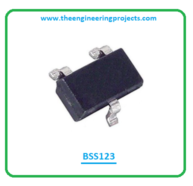
 Hi Guys! Hope you’re well today. Happy to see you around. In this post today, I’ll walk you through the Introduction to BSS123.
The BSS123 is an N-Channel Logic Level Enhancement Mode Field Effect Transistor that comes in surface mount package SOT-23. It is a rugged and reliable device that comes with a drain-source voltage of around 100V while the gate-source voltage is -+20V. It is mainly used in low voltage and low current applications like servo motor control and switching and amplificaiton applications.
I suggest you buckle up as I’ll detail the complete Introduction to BSS123 covering datasheet, pinout, features, and applications.
Let’s get started.
Introduction to BSS123
- The BSS123 is an N-Channel Logic Level Enhancement Mode Field Effect Transistor that comes in surface mount package SOT-23.
- This field-effect transistor is widely used in amplification and switching applications in a range of electronic devices.
- This is a three-terminal device with terminals named: gate, source, and drain. Sometimes, the body part is also considered as terminal, making it a four-terminal device.
- The drain current of this component is 170mA and it comes with a low threshold voltage of 1.7V.
- Know that the gate terminal is electrically insulated since it carries no current and is commonly called as Insulated Gate FET (IG-FET).
- There are two types of MOSFET i.e. N-channel MOSFET and P-channel MOSFET. This BSS123 chip falls under the category of N-channel MOSFET where electrons are the major charge carriers. In P-channel MOSFETs, holes are the major carrier.
- The movement of electrons is better than the movement of holes, so N-channel MOSFETs are better than P-channel MOSFETs and possess less resistance. The reason… with high loads the N-channel MOSFETs remain cool while P-channel MOSFET goes hot in the presence of high loads.
- The charge carriers (electrons in this case of N-channel MOSFET) enter the channel through the source terminal and leave the channel through the drain terminal.
- The gate terminal stands between the source and drain terminal and the voltage on the gate terminal controls the width of the channel.
- This N-channel MOSFET is commonly termed a transistor and is used in both digital and analog circuits.
- The operating temperature and storage junction temperature range of this device is -55C to 150C.
- The low on-state resistance makes this device the best pick for switching applications.
- The one drawback of this MOSFET is its low drain current. It offers a peak current of up to 1A at the maximum threshold voltage and a continuous current of 170mA.
- If you apply ratings more than the required absolute maximum ratings, it will damage the device.
BSS123 Datasheet
While working with this component in your electrical project, it’s wise to go through the datasheet of the component that features the main characteristics of the device. Click the link below to download the datasheet of BSS123.
BSS123 Pinout
The following figure represents the pinout diagram of BSS123.
This MOSFET carries three terminals gate, source, and drain.
| Pin Description of BSS123 | ||||
|---|---|---|---|---|
| Pin No. | Pin Description | Pin Name | ||
| 1 | Electrons enter the channel through Source | Source (S) | ||
| 2 | Controls the biasing of the MOSFET | Gate (G) | ||
| 3 | Electrons leave the channel through Drain | Drain (D) | ||
BSS123 Features
The following are the main features of BSS123.
- The resistance between drain and source terminal RDS (on-state resistance) is 6Ω at gate-source voltage VGS of 10V and it’s 10Ω at VGS of 4.5V.
- High-density cell design leads to extremely low on-state resistance RDS (ON).
- Drain Source Voltage (VDS) is 100V
- This chip is rugged and reliable.
- Comes in a compact industry-standard SOT-23 surface-mount package.
- The gate threshold voltage (VGS-th) is 1.7V typically
- Continuous Drain Current (ID) is 170mA
- Turn ON and Turn off delay time is 1.7ns and 17ns respectively
BSS123 Applications
This MOSFET device is used in the following applications.
- Used in automotive electronics.
- Incorporated in low voltage low current applications.
- Used in servo motor control.
- Employed as switching devices in electronic control units.
- Used as power converters in modern electric vehicles.
That’s all for today. Hope you find this article helpful. If you have any questions, you can pop your comment in the section below, I’d love to help you the best way I can. Feel free to share your valuable feedback and suggestions around the content we share so we keep coming back with quality content tailored to your exact needs and requirements. Thank you for reading the article.
JLCPCB – Prototype 10 PCBs for $2 (For Any Color)
China’s Largest PCB Prototype Enterprise, 600,000+ Customers & 10,000+ Online Orders Daily
How to Get PCB Cash Coupon from JLCPCB: https://bit.ly/2GMCH9w
The post BSS123 N-Channel MOSFET Datasheet, Pinout, Features & Applications appeared first on The Engineering Projects.


No comments:
Post a Comment